Semicon Global Tech
MEMS Foundry Services
MEMS processing
Lithography
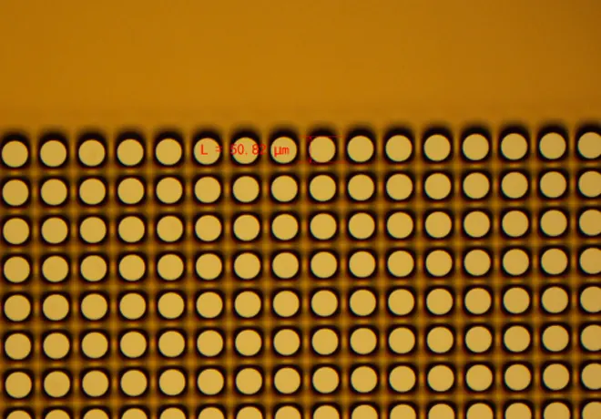
Lithography Overview
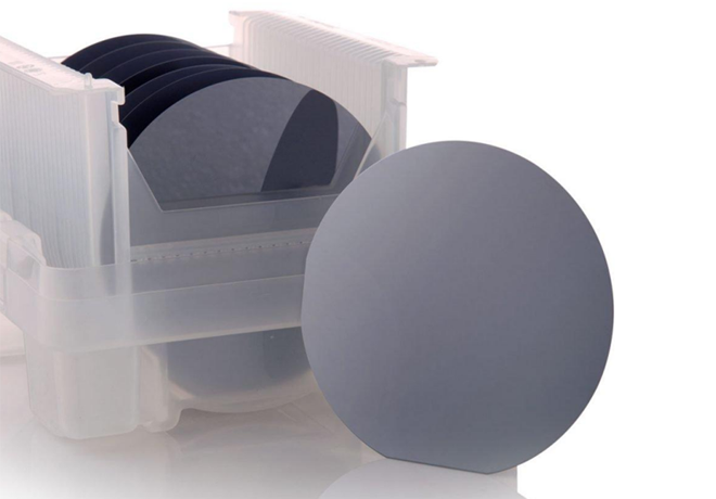
Lithography is an important step in semiconductor material manufacturing. It uses exposure and development to define geometric patterns in the photoresist layer, and then transfers the pattern from the photomask to the substrate through the etching process. Semicon Global Tech provides MEMS foundry services for universities and research institutes, with experience in multiple lithography technologies.
Applicable Materials
Silicon wafers, glass, sapphire, flexible materials and other substrates
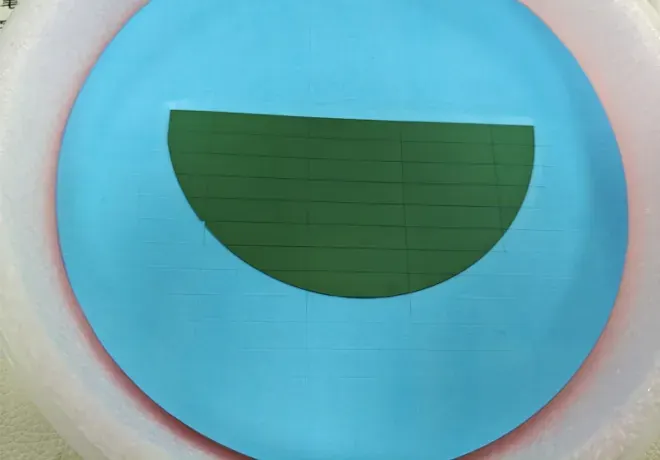
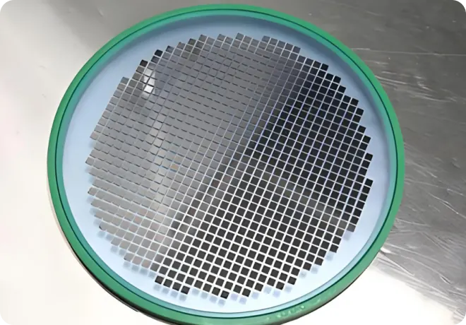
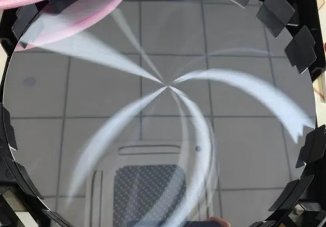
Lithography Technologies
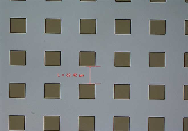
Contact Lithography Minimum feature size: 1 μm; overlay accuracy: ±0.5 μm
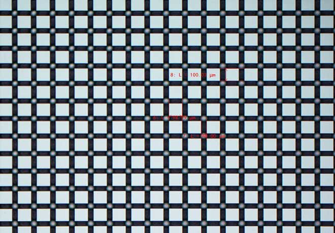
Stepper Lithography Projection ratio 1:5; minimum feature size: 0.35 μm; overlay accuracy ≤0.15 μm (X, Y); exposure range:<22 × 22 mm
Electron-Beam Lithography Minimum feature size: 10 nm; overlay accuracy: 40 nm; exposure range:<Φ100 mm
Learn More
MEMS代工
Etching
Etching Overview
Etching is the process of selectively removing unwanted materials from the surface of a silicon wafer by chemical or physical methods. It is a general term for stripping or removing materials through solutions, reactive ions or other mechanical methods. Etching technologies are mainly divided into dry etching and wet etching. Dry etching mainly uses reactive gases and plasma for etching, while wet etching relies on chemical reactions between chemical reagents and the material being etched. Semicon Global Tech provides MEMS foundry services for universities and research institutes, with experience in multiple etching methods.
Etching Chemicals
Alkaline KOH, TMAH
Acidic HF, BOE, HCl, HNO₃, etc.
Etchable Materials
Silicon, silicon oxide, silicon nitride, metals, quartz and other materials
Etching Technologies
Ion Beam Etching (IBE) Used for metals or other materials that are difficult to etch
Deep Silicon Etching (DRIE) Etching uniformity <±5%; selectivity >50:1
Reactive Ion Etching (RIE) Etching of Si, SiO₂, SiNx, etc.
Focused Ion Beam Etching (FIB) Micro/nano processing such as etching, deposition and doping can be performed on materials and devices.
Inductively Coupled Plasma (ICP) Etching Etching of GaN, GaAs, InP and other materials
Learn More
MEMS代工
Thin-Film Deposition
Thin-Film Deposition Overview
Thin-film deposition is a common surface treatment process. Generally performed in a vacuum environment, it deposits a metal or non-metal material onto the material surface in vapor phase to form a dense film. Film quality is critical to the functional formation of semiconductor devices. Semicon Global Tech provides MEMS foundry services for universities and research institutes, with experience in multiple thin-film deposition technologies.
Deposition Services
Oxide/nitride films, metal films, optical films, composite films, etc.
Film Materials
Metal materials Ti, Al, Ni, Au, Ag, Cr, Pt, Cu, Pd, Zn, Mo, W, Ta, Nb and other film materials
Non-metal materials Si, SiO₂, SiNx, Al₂O₃, HfO₂, MgF₂, Ta₂O₅, ITO and other film materials
Deposition Substrates
Substrate Silicon wafers, quartz glass wafers, sapphire wafers, PET, PI and other substrates
Substrate Size 2–8 inch
Film Thickness and Surface
Thickness Nanometer-level and micrometer-level thicknesses; customizable on request
Surface Single-side and double-side
Deposition Technologies
Electron-Beam Evaporation Ti,Al,Ni,Ag,Cu,Cr,Sn,Pt,AuGe
Magnetron Sputtering Ti、Al、Ni、Au、Ag、Cr、Pt、Cu、TiW90、Pd、Pt、Zn、Mo、W、Ta、Ru、Si、SiC、NiCr20、Nb
LPCVD (Low-Pressure Chemical Vapor Deposition) SiNx and poly-Si in-wafer uniformity: <±5%
PECVD (Plasma-Enhanced Chemical Vapor Deposition) SiO₂, SiNx, a-Si (B/P doped)
ALD Atomic Layer Deposition Al2O3、HfO2、AlN、ZrO2、SiO2、TiN、TiO2
Learn More
MEMS代工
Wafer Bonding
Wafer Bonding Overview
Wafer bonding is a technology in which two homogeneous or heterogeneous semiconductor materials with clean and atomically flat surfaces are directly joined after surface cleaning and activation. Under certain conditions, van der Waals forces, molecular forces or even atomic forces bond the wafers into an integrated structure. Semicon Global Tech provides MEMS foundry services for universities and research institutes, with experience in multiple wafer bonding technologies.
Anodic Bonding
Anodic Bonding A bonding technology assisted by an electric field
Applicable To Bonding between silicon and glass, metal and glass, semiconductor and alloy, and semiconductor and glass
Eutectic Bonding
Eutectic Bonding Also known as electrostatic bonding in some contexts, this process uses a low-melting-point alloy as an intermediate layer, such as Au-Sn alloy. When the alloy is heated to its eutectic point, the liquid metal fills microscopic recesses on the two material surfaces and forms a solid metal bond after cooling, enabling a strong connection.
Applicable To PbSn, AuSn, CuSn, AuSi and other materials
Adhesive Bonding
Adhesive Bonding Uses a specific adhesive to join two surfaces
Adopted Process AZ4620, SU-8 and other bonding adhesives
Applicable To 4 inch, 6 inch
Learn More
MEMS代工
Doping
Doping Overview
Doping introduces a specific amount and type of impurity into silicon and forms a precise impurity distribution profile. It can change the electrical properties of the wafer and realize the vertical structures of devices and circuits. Common methods include diffusion and ion implantation. High-temperature diffusion uses heat to drive impurities through the silicon crystal structure. Ion implantation uses high-energy ion bombardment to inject impurities into the silicon wafer through atomic-level high-energy collisions. Semicon Global Tech provides MEMS foundry services for universities and research institutes, with experience in ion implantation, diffusion, annealing and other semiconductor doping technologies.
Doping
Metal-Organic Chemical Vapor Deposition GaN,GaAs
Chemical Vapor Deposition SIC
Ion Implantation B,P,F,Al,N,Ar,H,He,Si
High-Temperature Oxidation
High-Temperature Diffusion / Annealing
Rapid Thermal Annealing
Learn More
MEMS代工
Dicing
Dicing Overview
Dicing, sometimes called wafer scribing, is an indispensable step in the chip manufacturing process and belongs to the back-end stage of wafer manufacturing. Its purpose is to separate each independent IC/MEMS on the wafer by laser or a high-speed rotating diamond blade, so that individual IC/MEMS devices can be attached, bonded and packaged in subsequent processes. Semicon Global Tech provides MEMS foundry services for universities and research institutes, with experience in laser dicing, blade dicing and other semiconductor dicing technologies.
Dicing Methods
Laser Dicing Silicon substrates
Thickness 100-700μm
Wafer Size 2 inch, 4 inch, 6 inch, 8 inch

Blade Dicing Dicing of Si, Ge, glass, quartz, ceramics and circuit boards
Applicable Materials
2–8 inch wafers
Scribing and dicing of metal materials, silicon, germanium, gallium arsenide and other semiconductor substrate materials
Dicing of glass, quartz, ceramics and circuit boards
Learn More
MEMS代工
Micro Drilling
Micro Drilling Overview
Micro drilling is an indispensable step in chip manufacturing. It can form through-holes on chips for through-conductors or structural components. Chip and metal drilling technologies are mainly divided into mechanical drilling and laser drilling. Semicon Global Tech provides MEMS foundry services for universities and research institutes, and offers micro-hole drilling services for glass, metal sheets, silicon wafers, semiconductors and chips.
Materials and Services
Material Glass, metal sheets, silicon wafers, semiconductors, chips and related materials
Micron-scale holes Micro-hole drilling processing service is available
Learn More
MEMS代工
Wafer Thinning
Wafer Thinning Overview
Before wafer packaging, excess substrate material on the wafer backside usually needs to be removed to a certain thickness; this process is called wafer thinning. In the back-end process, wafers with circuits already formed on the front side undergo backside thinning before subsequent dicing, wire bonding and packaging. This reduces packaging and mounting height, decreases chip package volume, improves heat dissipation efficiency, electrical performance and mechanical performance, and reduces the workload for dicing. Semicon Global Tech provides MEMS foundry services for universities and research institutes, with experience in mechanical grinding, chemical mechanical polishing and other semiconductor wafer thinning technologies.
Wafer Thinning Technologies
Wafer Thinning Technologies Mechanical grinding, chemical mechanical polishing and related processes
Applicable Materials
Applicable Materials Si, GaAs, GaN, InP, glass, sapphire, ceramics, etc.
Uniformity
Uniformity ±2um
Learn More
MEMS代工
Polishing
Polishing Overview
Polishing uses mechanical, chemical or electrochemical action to reduce the surface roughness of wafers and other workpieces, producing a bright and flat surface. It modifies the workpiece surface using polishing tools, abrasive particles or other polishing media. Semicon Global Tech provides MEMS foundry services for universities and research institutes, with experience in mechanical polishing, chemical polishing, chemical mechanical polishing and other wafer and semiconductor polishing technologies.
Polishing Technologies
Polishing Technologies Mechanical polishing, chemical polishing, chemical mechanical polishing and related processes
Applicable Materials
Applicable Materials Si, GaAs, GaN, InP, glass, sapphire, ceramics, etc.
Surface Roughness
Surface Roughness 1-50nm
Learn More
MEMS代工
Electroplating
Electroplating Overview
Electroplating uses chemical methods to deposit precious metals on specific electrodes. Its basic principle is similar to conventional electroplating, but it offers higher precision and control. Electroless plating refers to the deposition of metal ions from an aqueous solution onto a substrate through chemical reduction under controlled conditions without applying an external current. Semicon Global Tech provides MEMS foundry services for universities and research institutes, with experience in micro-electroplating, electroless plating and related electroplating processes.
Electroplating Technologies
Wafer-Level Electroplating Au,Cu,Ni,Sn
Micro-electroforming for non-standard sizes Electroplating of Au, Cu and Ni is available on non-standard sizes and flexible substrates
Electroless Ni/Pd/Au Plating
Learn More
MEMS代工
Copyright © © Semicon Global Tech Co., Ltd. All Rights Reserved.