Wafer Thinning
Wafer Thinning Overview
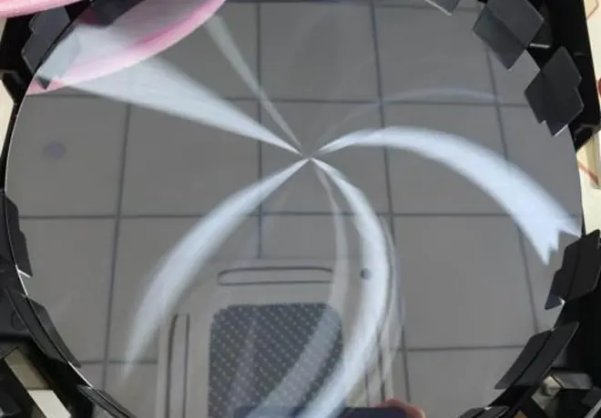
Before wafer packaging, a certain thickness of excess substrate material usually needs to be removed from the back side of the wafer. This process is called wafer thinning. In the back-end process stage, wafers with circuits already formed on the front side are thinned from the back before subsequent dicing, wire bonding and packaging. Thinning helps reduce package mounting height, decrease chip package volume, improve thermal diffusion efficiency, electrical performance and mechanical performance, and reduce the amount of dicing work. Semicon Global Tech provides MEMS foundry services and supports semiconductor wafer and chip thinning technologies such as mechanical grinding and chemical mechanical polishing.
Wafer Thinning Technologies
Mechanical grinding, chemical mechanical polishing and related thinning processes.
Applicable Materials
Si, GaAs, GaN, InP, glass, sapphire, ceramics and other compatible substrate materials.
Uniformity
Uniformity: ±2 μm