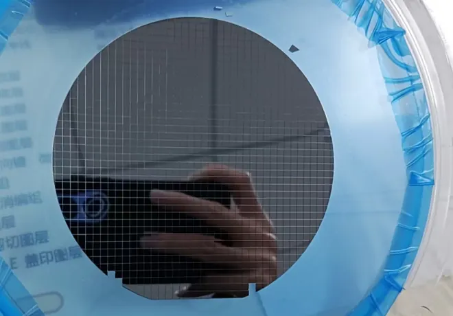
Dicing Overview
Dicing is sometimes also called scribing. It is an indispensable process in chip manufacturing and belongs to the back-end stage of wafer fabrication. The purpose of dicing is to separate each independent IC or MEMS device on the wafer by laser or high-speed rotating diamond blade, so that individual IC/MEMS devices can be attached, bonded and packaged in subsequent processes. Semicon Global Tech provides MEMS foundry services and is experienced in laser dicing, blade dicing and other semiconductor dicing technologies.
Applicable Materials
2–8 inch wafers; dicing and cutting of metal materials, silicon, germanium, gallium arsenide and other semiconductor substrate materials; glass, quartz, ceramics and circuit boards.