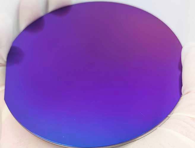
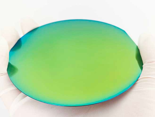
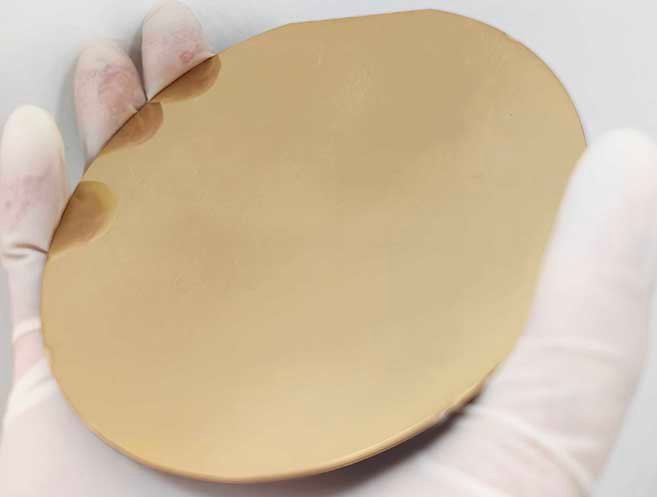
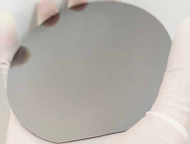
| Metals | Ti, Al, Ni, Au, Ag, Cr, Pt, Cu, Pd, Zn, Mo, W, Ta, Nb and other metal coating materials |
| Non-metals | Si, SiO₂, SiNₓ, Al₂O₃, HfO₂, MgF₂, Ta₂O₅, ITO and other non-metal coating materials |
| Substrates | Silicon wafers, quartz glass wafers, sapphire wafers, PET, PI and other substrates |
| Substrate Size | 2–8 inches |
| Thickness | Nanometer-level and micrometer-level thicknesses; customizable on request |
| Surface | Single-sided or double-sided deposition |
| Electron-Beam Evaporation | Ti, Al, Ni, Ag, Cu, Cr, Sn, Pt, AuGe |
| Magnetron Sputtering | Ti, Al, Ni, Au, Ag, Cr, Pt, Cu, TiW90, Pd, Pt, Zn, Mo, W, Ta, Ru, Si, SiC, NiCr20, Nb |
| LPCVD (Low-Pressure Chemical Vapor Deposition) | SiNₓ, Poly-Si; wafer-level uniformity: <±5% |
| PECVD (Plasma-Enhanced Chemical Vapor Deposition) | SiO₂, SiNₓ, a-Si (B/P doped) |
| ALD (Atomic Layer Deposition) | Al₂O₃, HfO₂, AlN, ZrO₂, SiO₂, TiN, TiO₂ |