Semicon Global Tech
Wafer Bonding
MEMS Foundry Services
MEMS processing
Wafer Bonding
Wafer Bonding Overview
Wafer bonding joins two clean, atomically flat homogeneous or heterogeneous semiconductor material surfaces after surface cleaning and activation. Under controlled conditions, the wafers are bonded into an integrated structure through van der Waals forces, molecular forces or even atomic forces. Semicon Global Tech provides MEMS foundry services and has experience with multiple wafer bonding technologies.
Anodic Bonding
Anodic BondingAn electric-field-assisted bonding technologySuitable forBonding between silicon wafers and glass, metal and glass, semiconductors and alloys, and semiconductors and glass
Eutectic BondingAlso known as electrostatic bonding in some process contexts. It uses a low-melting-point alloy as an intermediate layer, such as gold-tin (Au-Sn). When heated to the eutectic temperature, the liquid metal fills microscopic surface recesses and forms a solid metal bond after cooling, creating a strong connection.Suitable forPbSn, AuSn, CuSn, AuSi and related material systems
Adhesive BondingUses selected bonding adhesives to connect two surfaces.AdhesivesAZ4620, SU-8 and other dedicated bonding adhesives
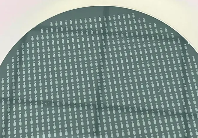
Applicable wafer sizes4-inch and 6-inch wafers
Eutectic Bonding
Eutectic bonding uses metal alloy systems such as AuSn, PbSn, CuSn or AuSi to form a stable bonded interface at controlled temperature.
Adhesive Bonding
Adhesive bonding uses materials such as AZ4620 or SU-8 to join two wafer or substrate surfaces for MEMS packaging and structure integration.
Case Studies
Copyright © © Semicon Global Tech Co., Ltd. All Rights Reserved.